- Home
- Physical Design Trainings
100% Job Oriented VLSI Trainings
VLSI Physical Design Trainings
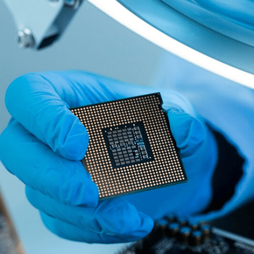
Physical Design course is designed to provide students with a comprehensive understanding of the key principles, methodologies, and techniques required to design and optimize integrated circuits at the physical level. This course is essential for electrical and electronics engineering students, semiconductor professionals, and anyone interested in the field of semiconductor manufacturing and chip design.

Online/Offline Trainings
Expert instructos
100% Placement Rate
Eligibility Criteria
- B.Tech/M/Tech degree in Electronics & Communication (ECE), Electrical & Electronics (EEE), or closely related fields.
- B,Tech/M.Tech in Computer Science (CSE) or Closely related Fields
- M.Tech in VLSI or closely related fields
Course Curriculum
Module 1 :VLSI Physical Design Digital Electronics
- Logic Gates
- Boolean Algebras, Boolean Expression and K-Map
- Combinational Circuits
Adders, Subtractors, Multiplexer, Demultiplexer, Encoders, Priority Encoder, Decoders, Comparator, and converters.
- Sequential Circuits : Latches, Flip-Flops, Registers and Counters
Assignment and Mock Interview
Module 2 : CMOS
- Introduction to MOSFET, CMOS Inverter and its characteristics
- CMOS Logic and Stick Diagrams
- Fabrication Process, Second Order Effects and Latch up
Assignment and Mock Interview
Module 3 : LINUX
- Introduction of Linux/Unix
- Utilities of Linux and Unix OS
- Basic commands
- File Permission in Linus/Unix
- Regular expression
- Environmental Variables
- Process Management
Assignment and Mock Interview
Module 4 : TCL
- Introduction
- Special Variables
- Basic Syntax
- Data Types
- Variables
- Operators
- Decisions
- Loops
- Arrays
- Strings
- Lists
- Dictionary
- Procedures
- Packages
- Files I/O
- Regular Expressions
Assignment and Mock Interview
Module 5 : STA
- Introduction to STA
- What is Timing Analysis
- Types of STA
- Advantages of STA
- Inputs and Outputs of STA
- Terminologies in STA
- Slew, Delay in Circuits
- Setup and Hold time
- Timing arcs
- Problems on slew and delay
- Timing Path Groups
- Terminologies related to path groups
- Problems on Path groups
- Clocks
- Pulse width
- Period
- Frequency
- Duty Cycle
- Edges
- Clock Abnormalities
- Timing Exceptions and Time borrowing concept
- PVT conditions, OCV, CRPR and Problems
- Timing Reports and fixing the timing violations
- Signal Integrity
Assignment and Mock Interview
Module 6 : Physical Design
- ASIC flow and Synthesis
- PD flow
- Design setup
- Library
- DEF
- SPEF
- Netlist
- SDC
- LEF
- UPF
Test and Mock Interview
- Floor planning
- Defining the chip/die/core area
- Placing the pin or IO placement
- Macro placement
- Adding blockages/defining the placement and routing blockages
- Power planning
- Placement
- Goals for placement optimization
- Intermediate steps in placement optimization
- Analysis and debug
- CTS
- Pre-CTS checks
- Goals for CTS
- Post-CTS optimization
- Routing
- Global routing
- Track assignments
- Detail routing
Assignment and Mock Interview
Module 7 : Physical Verification
- Inputs
- DRC
- LVS
- PERC
- Softcheck
- XoR
- Antenna
- DFM
Assignment and Mock Interview
- Next Batch Commencing ON :January 10th, 2025
- Connect with us to schedule a demo Class
Register Now and Get a 25% Discount
People Love To Learn With US.
9/10
outcomes.
85%
85% of students Changed their Domain From IT to VLSI through SuccessBridge
Good Institute to start Career

Adhil Sinan
Get ready for good Career Growth

Mohit Kaur
Excellent Trainer Support


