Introduction
When it comes to designing integrated circuits or chips, there are several critical steps in the process, each with its own unique importance. One of these fundamental steps is “floorplanning.” Floorplanning is the initial stage in chip design, where engineers lay the groundwork for the physical layout of the components on the chip. In this blog post, we will delve into what floorplanning is, why it matters, and how it influences the success of a chip design project.
What Is Floorplanning?
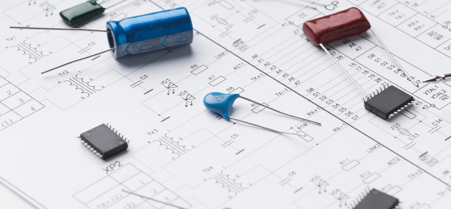
At its core, floorplanning is the process of determining the physical arrangement of various components and functional blocks on a semiconductor chip. Think of it as designing the blueprint for a city before constructing the buildings. The goal of floorplanning is to optimize the chip’s physical layout for factors such as performance, power efficiency, and manufacturability.
Key Aspects of Floorplanning
- Component Placement: Engineers decide where each functional block, such as processors, memory, input/output interfaces, and more, will be located on the chip. Proper placement is crucial for minimizing signal delays, reducing power consumption, and ensuring efficient heat dissipation.
- Wiring Architecture: Floorplanning includes planning for the routing of wires and interconnections between components. Efficient wiring architecture is vital to maintain signal integrity and avoid bottlenecks that can hinder chip performance.
- Power and Heat Management: Engineers must consider power distribution and thermal management during floorplanning. Proper placement of power supplies, voltage regulators, and heat sinks is essential to ensure the chip operates within safe temperature limits.
- Signal Timing: Floorplanning plays a significant role in meeting timing constraints. By carefully placing components and routing signals, designers can minimize signal propagation delays and ensure that the chip operates at the required clock speeds.
Why Floorplanning Matters
- Performance Optimization: A well-executed floorplan can significantly impact the performance of a chip. It allows for shorter interconnect lengths, reduced signal delays, and improved overall efficiency.
- Power Efficiency: Proper floorplanning can lead to lower power consumption by minimizing unnecessary wire lengths and optimizing power distribution.
- Manufacturability: An efficient floorplan is easier to manufacture, reducing production costs and improving yield rates.
- Time-to-Market: Effective floorplanning can accelerate the design process, helping companies bring their products to market more quickly.
- Cost Reduction: By optimizing the chip’s layout, floorplanning can lead to cost savings in terms of materials, manufacturing, and testing.
Conclusion
In the complex world of chip design, floorplanning serves as the foundational step that sets the stage for the entire project. It is a meticulous process that involves careful consideration of performance, power, and manufacturability. An effective floorplan can be the difference between a successful chip and one that falls short of expectations.
As technology continues to advance, floorplanning tools and methodologies are evolving to meet the demands of ever more complex semiconductor designs. Engineers and designers must continually refine their skills in this critical area to create chips that meet the high-performance standards of today’s electronic devices.


