Latch-Up in VLSI: Navigating the Currents of Reliability in Semiconductor Design
Introduction:
Very Large Scale Integration (VLSI) has been a driving force behind the incredible advancements in modern electronics. As semiconductor technology continues to evolve, designers face the challenge of ensuring the reliability and robustness of integrated circuits. One critical aspect that demands attention is latch-up, a phenomenon that can have significant consequences if not properly understood and mitigated.
What is Latch-Up?
Latch-up in VLSI is a condition in integrated circuits (ICs) where a low-impedance path is formed between the power supply rails, leading to a sustained and self-sustaining current flow. This can cause the device to malfunction or even fail, posing a serious threat to the reliability of the entire system.
Understanding Latch-Up Mechanism:
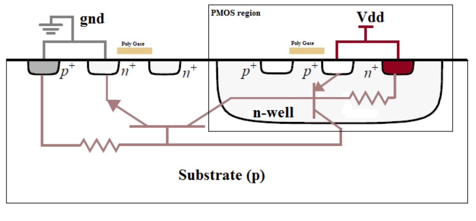
Latch-up is primarily a result of the interaction between parasitic bipolar transistors present in the semiconductor substrate. These parasitic structures can inadvertently turn on and create a short circuit between the power supply rails. The triggering of latch-up is often influenced by external factors such as high voltage, high current, or even radiation.
Key Components of Latch-Up:
- Parasitic Bipolar Junction Transistors (BJTs):
- These are unintentional bipolar transistors formed due to the inherent structure of the IC.
- NPN and PNP parasitic transistors can form unintentional circuits leading to latch-up.
- SCR (Silicon-Controlled Rectifier):
- Latch-up can be described as the turning on of an SCR structure, which is formed by the parasitic BJTs.
- Once triggered, the SCR remains latched until external intervention.
Preventing Latch-Up:
- Well-Designed Layout:
- Proper layout design, including guard rings and isolation techniques, can minimize the risk of latch-up.
- Ensuring a balanced distribution of N-wells and P-wells is crucial.
- Power Supply Decoupling:
- Decoupling capacitors can help in maintaining stable power supplies, preventing sudden voltage spikes that may trigger latch-up.
- Reducing Parasitic Capacitance:
- Minimizing the parasitic capacitance in the layout can reduce the likelihood of latch-up.
- Strategic placement of diffusion layers and optimizing the interconnect structure are essential.
- Latch-Up Testing:
- Rigorous testing during the design phase can help identify potential latch-up issues.
- Techniques like Current-Voltage (IV) testing can reveal susceptibility to latch-up.
Conclusion:
In the ever-evolving field of VLSI, understanding and addressing latch-up is essential to ensure the reliability and longevity of integrated circuits. As technology continues to advance, designers must stay vigilant in implementing robust design practices, leveraging simulation tools, and conducting thorough testing to mitigate the risks associated with latch-up. By doing so, the VLSI community can continue pushing the boundaries of what is possible in the realm of semiconductor technology.
To know more about VLSI Course , SuccessBridge VLSI training institute. You can begin your VLSI career by enrolling in the placement-assisted live courses available at SuccessBridge We offer various VLSI online courses. We offer VLSI Physical Design course, Design Verification course, DFT Training,Chip design course many more. Explore VLSI Courses From The Leaders In VLSI Training
Also Read: A Walkthrough VLSI Physical Design Engineer Salary In India.