Unveiling the Essentials to Become a DFT Engineer in India’s Semiconductor Landscape.
Introduction
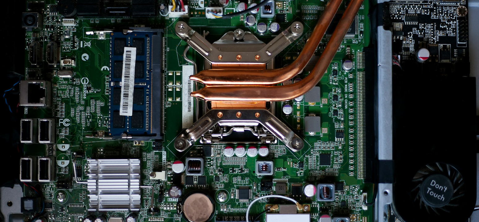
In the ever-evolving realm of semiconductor design, the role of a VLSI DFT (Very Large Scale Integration Design for Testability) engineer is indispensable. As the demand for complex and high-performance integrated circuits continues to soar, the need for skilled professionals in the field of VLSI DFT becomes more critical than ever. This blog aims to shed light on the key aspects of VLSI DFT, providing valuable insights for aspiring engineers looking to carve a niche in this exciting domain.
- Essentials of VLSI DFT: Laying the Foundation
- Begin by unraveling the foundational concepts of VLSI design, digital logic, and testing methodologies.
- Familiarize yourself with industry-standard tools such as Cadence Encounter Test and the Mentor Graphics Tessent suite.
- Role and Responsibilities of a VLSI DFT Engineer: Orchestrating Testability
- Dive into the critical role VLSI DFT engineers play in ensuring the manufacturability and reliability of integrated circuits.
- Explore responsibilities like implementing testability features, designing scan chains, and developing fault models for robust test pattern generation.
- Mastering Scan Chain Implementation: The Backbone of DFT
- Gain expertise in designing efficient scan chains, covering scan flip-flops, shift and capture cycles, and understanding the impact of scan chain length on test time.
- Test Pattern Generation Techniques: Art and Science
- Delve into the art of creating effective test patterns using various algorithms and techniques.
- Explore automatic test pattern generation (ATPG) and fault simulation, emphasizing the balance between high fault coverage and minimal test time.
- Fault Models and Simulation: Decoding Defects
- Understand common fault models, including stuck-at faults and transition faults, and their role in identifying defects.
- Explore fault simulation techniques to validate the efficacy of test patterns.
- Emerging Trends Shaping VLSI DFT: Navigating the Future
- Stay ahead of the curve by exploring the latest trends, such as the integration of machine learning in test pattern generation.
- Discuss the impact of 3D integration on testing strategies and the evolving role of DFT in ensuring security in integrated circuits.
- Advanced Techniques and Innovations: Pushing the Boundaries
- Explore advanced techniques and innovations in VLSI DFT, including the utilization of on-chip instrumentation and self-test techniques.
- Understand how built-in self-test (BIST) and concurrent test strategies contribute to enhancing testability.
Conclusion: As you embark on your journey in VLSI DFT engineering, remember that the landscape is ever-evolving. This deep dive into the intricacies of design-for-test engineering equips you with the knowledge and skills needed to navigate this dynamic field. With innovation as your compass, you’ll be well-prepared to contribute to the advancement of semiconductor design, ensuring the reliability and testability of the integrated circuits shaping our technological future.
To know more about VLSI Course , SuccessBridge VLSI training institute. You can begin your VLSI career by enrolling in the placement-assisted live courses available at SuccessBridge We offer various VLSI online courses. We offer VLSI Physical Design course, Design Verification course, DFT Training,Chip design course many more. Explore VLSI Courses From The Leaders In VLSI Training
Also Read: A Walkthrough VLSI Physical Design Engineer Salary In India.


