Introduction:
Welcome to the fascinating world of Very Large Scale Integration (VLSI) fabrication, where the intricate dance of electrons and silicon come together to create the heart of modern electronic devices. In this blog post, we will embark on a journey through the complex and precise process of VLSI fabrication, shedding light on the various stages that transform raw materials into powerful microchips.
Stage 1: Design and Mask Creation
The VLSI fabrication process kicks off with meticulous design planning. Engineers and designers collaborate to create a blueprint of the integrated circuit (IC), defining the arrangement of transistors, interconnects, and other components. This blueprint is then translated into a set of masks, essentially the stencils that guide subsequent manufacturing steps.
Stage 2: Silicon Wafer Preparation
The heart of VLSI fabrication lies in the silicon wafer. These wafers, often 12 inches in diameter, undergo a series of cleaning and preparation steps. A thin layer of silicon dioxide, known as the oxide layer, is grown or deposited on the wafer’s surface, providing insulation and protection.
Stage 3: Photolithography
Photolithography is a pivotal step where the mask patterns are transferred onto the silicon wafer. Ultraviolet light is used to expose the wafer through the masks, creating a photoresist pattern. This pattern serves as a guide for subsequent etching and deposition processes.
Stage 4: Etching and Deposition
Etching involves removing unwanted material from the wafer, leaving only the desired pattern. Chemicals or plasma are commonly used in this step. Deposition follows, where new material is added to the wafer’s surface, contributing to the formation of various layers.
Stage 5: Doping
Doping introduces specific impurities into the silicon to alter its electrical properties. This step is crucial for creating transistors with distinct characteristics. The choice of dopants and their concentration significantly impacts the performance of the integrated circuit.
Stage 6: Metallization and Interconnection
Metallization involves the deposition of metal layers, typically aluminum or copper, to establish interconnections between different components on the chip. These metal layers form the intricate wiring that enables communication between transistors and other elements.
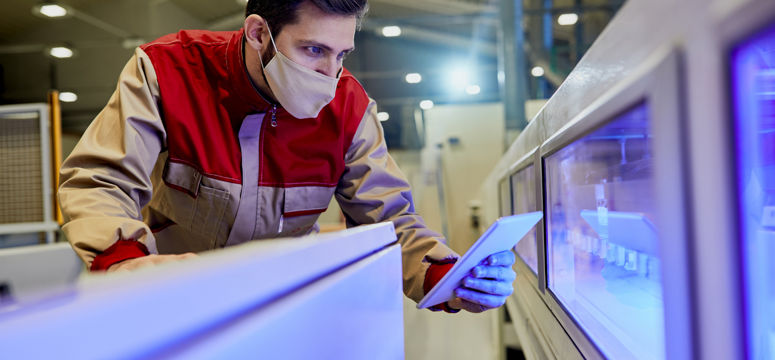
Stage 7: Testing and Quality Assurance
Once the fabrication process is complete, rigorous testing is conducted to ensure the functionality and reliability of the integrated circuits. Defective chips are identified and discarded during this phase to maintain high-quality standards.
Conclusion:
The VLSI fabrication process is a symphony of precision and innovation, weaving together advanced technology and scientific principles. As we continue to push the boundaries of miniaturization and efficiency, the world of VLSI fabrication remains at the forefront of technological advancements, shaping the future of electronics. Stay tuned for more insights into the ever-evolving realm of semiconductor manufacturing!
Also Read: A Walkthrough VLSI Physical Design Engineer Salary In India.
To know more about VLSI Course , SuccessBridge VLSI training institute. You can begin your VLSI career by enrolling in the placement-assisted live courses available at SuccessBridge We offer various VLSI online courses. We offer VLSI Physical Design course, Design Verification course, DFT Training,Chip design course many more. Explore VLSI Courses From The Leaders In VLSI Trainin


