Introduction:
In the ever-evolving realm of Very Large Scale Integration (VLSI) design, engineers grapple with numerous challenges to ensure the seamless functioning of intricate electronic circuits. One such challenge that often demands a closer look is crosstalk—a phenomenon that can significantly impact the performance and reliability of integrated circuits. In this blog post, we delve into the depths of crosstalk in VLSI, exploring its origins, implications, and mitigation strategies.
Understanding Crosstalk:
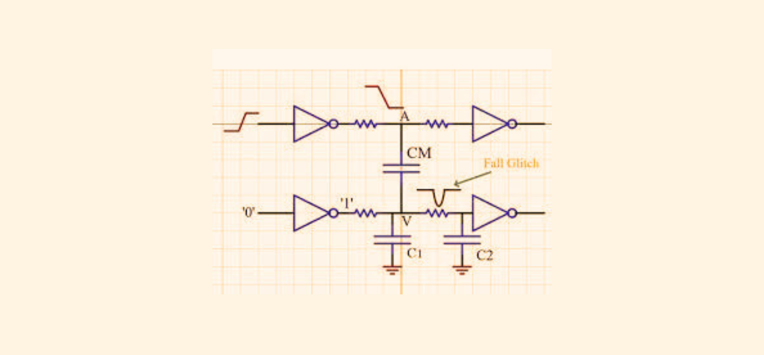
Crosstalk, in the context of VLSI, refers to the unwanted interference between adjacent signal lines on a chip. This interference occurs when the signals on one line induce an undesired voltage in an adjacent line, leading to signal distortion and potential data corruption. As chip designs become more compact and intricate, crosstalk emerges as a critical consideration for VLSI designers.
Origins of Crosstalk:
The primary sources of crosstalk in VLSI are capacitive and inductive coupling between adjacent conductors. Capacitive coupling occurs due to the electric field between closely spaced conductors, while inductive coupling arises from the magnetic field generated by current flow in adjacent lines. These phenomena intensify as signal frequencies increase, underscoring the importance of crosstalk management in high-speed VLSI circuits.
Implications for VLSI Circuits:
The repercussions of crosstalk in VLSI circuits are far-reaching. Signal integrity is compromised as distorted signals can lead to erroneous data transmission. Additionally, increased power consumption may result from the need to boost signal strength to overcome crosstalk-induced losses. In worst-case scenarios, crosstalk can contribute to the overall degradation of the chip’s performance and reliability.
Mitigation Strategies:
VLSI designers employ various strategies to mitigate the impact of crosstalk and ensure optimal circuit performance. Some common approaches include:
- Spacing and Arrangement: Proper spacing and arrangement of signal lines help minimize capacitive and inductive coupling. Designers carefully plan the layout to reduce the likelihood of interference between adjacent conductors.
- Shielding Techniques: Introducing shielding layers or metal shields between critical signal lines can help mitigate crosstalk by containing the electric and magnetic fields.
- Buffer Insertion: Buffer insertion involves strategically placing buffer stages along signal lines to strengthen signals and counteract the effects of crosstalk.
- Twisted Pair Routing: Employing twisted pair routing for critical signal lines helps reduce inductive coupling, as the magnetic fields generated by the currents in each wire tend to cancel each other out.
Conclusion:
In the intricate landscape of VLSI design, crosstalk emerges as a formidable challenge that demands meticulous attention. By understanding the origins and implications of crosstalk and implementing effective mitigation strategies, VLSI designers can pave the way for the creation of high-performance integrated circuits. As technology continues to advance, the ongoing quest for innovative solutions to crosstalk-related challenges remains a pivotal aspect of VLSI design.
To know more about VLSI Course , SuccessBridge VLSI training institute. You can begin your VLSI career by enrolling in the placement-assisted live courses available at SuccessBridge We offer various VLSI online courses. We offer VLSI Physical Design course, Design Verification course, DFT Training,Chip design course many more. Explore VLSI Courses From The Leaders In VLSI Training
Also Read: A Walkthrough VLSI Physical Design Engineer Salary In India.


