Introduction
The world of Very Large Scale Integration (VLSI) has witnessed remarkable advancements in recent years. As integrated circuits become increasingly complex and dense, ensuring their functionality and reliability has become a critical challenge. This is where the Design Verification and Validation (DV&V) process comes into play. In this blog post, we will explore the significance of DV&V in the VLSI domain and delve into the key steps and methodologies involved in this essential phase of chip design.
Understanding DV&V in VLSI
Design Verification and Validation are two distinct yet closely related processes that are integral to VLSI design. These processes aim to confirm that a semiconductor chip functions as intended, meets performance specifications, and is free of defects or errors.
- Design Verification (DV):
DV primarily focuses on answering the question, “Did we design the chip correctly?” It is the process of rigorously testing the design against a set of predefined specifications and requirements. The primary objective is to verify that the chip design behaves as expected under various operating conditions.
Key Steps in DV:
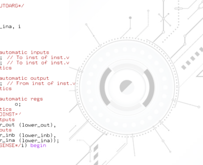
a. Testbench Development: Designers create a testbench, a set of test cases, and stimuli that mimic real-world scenarios to verify the chip’s functionality.
b. Simulation: The chip design is subjected to extensive simulations to ensure it meets performance, power, and area requirements.
c. Formal Verification: Formal methods such as model checking and theorem proving are used to mathematically prove the correctness of the design.
d. Code Review: Design code and scripts are reviewed for adherence to coding standards and best practices.
e. Functional Verification: Various techniques, including random testing, directed testing, and assertion-based verification, are employed to ensure the chip functions correctly.
- Design Validation (VAL):
While DV ensures that the chip has been designed correctly, Design Validation answers the question, “Did we design the right chip?” It focuses on verifying that the chip meets market and customer requirements and is suitable for its intended application.
Key Steps in VAL:
a. Silicon Validation: Once the chip is fabricated, it is physically tested to ensure it meets the specified performance, power, and reliability criteria. This step often involves ATE (Automatic Test Equipment) and may include in-system testing.
b. Emulation and Prototyping: Before fabrication, emulation and prototyping tools are used to validate the chip’s functionality in a hardware environment.
c. System-Level Testing: The chip is tested in the context of the larger system to ensure compatibility and performance under real-world conditions.
Benefits of Design Verification &Validation in VLSI
- Reduced Development Time: Early detection and resolution of design issues through DV&V save time in the long run by minimizing costly redesigns and rework.
- Improved Quality: Rigorous testing and validation processes enhance the reliability and quality of semiconductor chips, reducing the likelihood of field failures.
- Cost Savings: Identifying and fixing design issues during the DV&V phase is far less expensive than addressing them after fabrication.
- Compliance Assurance: Ensures compliance with industry standards and customer requirements, enhancing market acceptance.
- Risk Mitigation: DV&V reduces the risks associated with complex chip designs and semiconductor fabrication.
Conclusion
Design Verification and Validation are indispensable phases in the VLSI design process. They ensure that semiconductor chips are not only designed correctly but are also fit for their intended purposes. The increasing complexity of integrated circuits makes DV&V processes more critical than ever, as they play a pivotal role in delivering reliable and high-quality chips to meet the demands of modern electronics.
if you’re aspiring to master design verification in the field of VLSI, SuccessBridge stands out as the premier choice for training and education. With their top-notch VLSI training programs, you can gain the knowledge and hands-on experience needed to excel in design verification and make a significant impact in the world of digital design. Don’t miss the opportunity to join SuccessBridger, where your path to success in VLSI design verification begins.
In the dynamic world of VLSI, DV&V is the cornerstone of chip design, helping semiconductor companies stay competitive, innovate, and deliver cutting-edge technology to consumers across the globe.