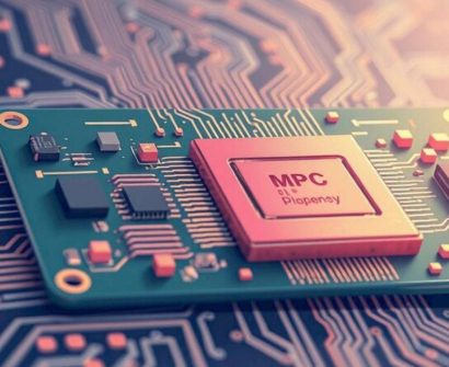
Introduction to FPGA in VLSI
Field-Programmable Gate Arrays (FPGAs) have become a cornerstone of modern VLSI design, offering flexibility, speed, and power efficiency. Unlike ASICs, which are custom-built for specific applications, FPGAs allow engineers to reconfigure their design post-fabrication, making them ideal for prototyping, research, and dynamic applications.
Why Use FPGAs in VLSI Design?
FPGAs provide several advantages in VLSI design:
- Reconfigurability: Designers can modify the hardware logic without fabricating a new chip.
- Parallel Processing: Multiple operations can be executed simultaneously, improving performance.
- Shorter Time to Market: Prototyping and testing are quicker compared to ASICs.
- Cost-Effectiveness: Lower non-recurring engineering (NRE) costs make FPGAs suitable for startups and small-scale applications.
FPGA Architecture Overview
FPGAs consist of several key components:
- Configurable Logic Blocks (CLBs): The fundamental units that implement logic functions.
- Interconnects: Programmable pathways that allow data transfer between CLBs.
- Input/Output Blocks (IOBs): Manage communication with external devices.
- Memory Elements: Embedded RAM blocks store intermediate data.
- Clocking Resources: Provide synchronization and timing control.
FPGA Design Flow
The FPGA design process follows these key steps:
- Specification & Requirement Analysis: Define system functionality and performance expectations.
- Design Entry: Use hardware description languages (HDLs) like VHDL or Verilog to describe circuit behavior.
- Synthesis: Convert HDL code into a netlist representing logic gates.
- Implementation: Perform placement and routing to map logic onto FPGA resources.
- Bitstream Generation: Compile the design into a file that programs the FPGA.
- Testing & Verification: Use simulations and real-time debugging to ensure functionality.
FPGA vs. ASIC: Key Differences
| Feature | FPGA | ASIC |
|---|---|---|
| Customization | Reconfigurable | Fixed design |
| Performance | Lower than ASICs | Optimized for speed and power |
| Cost | High per-unit, low NRE | Low per-unit, high NRE |
| Time to Market | Short | Long |
Applications of FPGA in VLSI
FPGAs are widely used in:
- Telecommunications: Signal processing, modulation, and error correction.
- Automotive: ADAS, real-time monitoring, and in-vehicle networking.
- Aerospace & Defense: Radar systems, encryption, and secure communications.
- AI & Machine Learning: Accelerating neural networks and AI workloads.
- Consumer Electronics: High-performance gaming, graphics, and IoT applications.
Future Trends in FPGA Design
The FPGA landscape is evolving with:
- AI and ML Integration: FPGAs are increasingly used for deep learning acceleration.
- Edge Computing: Enhancing real-time processing capabilities at the device level.
- Quantum Computing Support: Emerging FPGA architectures assist in quantum simulations.
- Low-Power Optimization: Advances in power-efficient FPGA architectures.
Conclusion
FPGA-based design plays a crucial role in modern VLSI, bridging the gap between flexibility and performance. Whether for prototyping, real-time processing, or AI acceleration, FPGAs offer unparalleled advantages in the semiconductor industry. As technology advances, FPGAs will continue to push the boundaries of innovation in VLSI design.