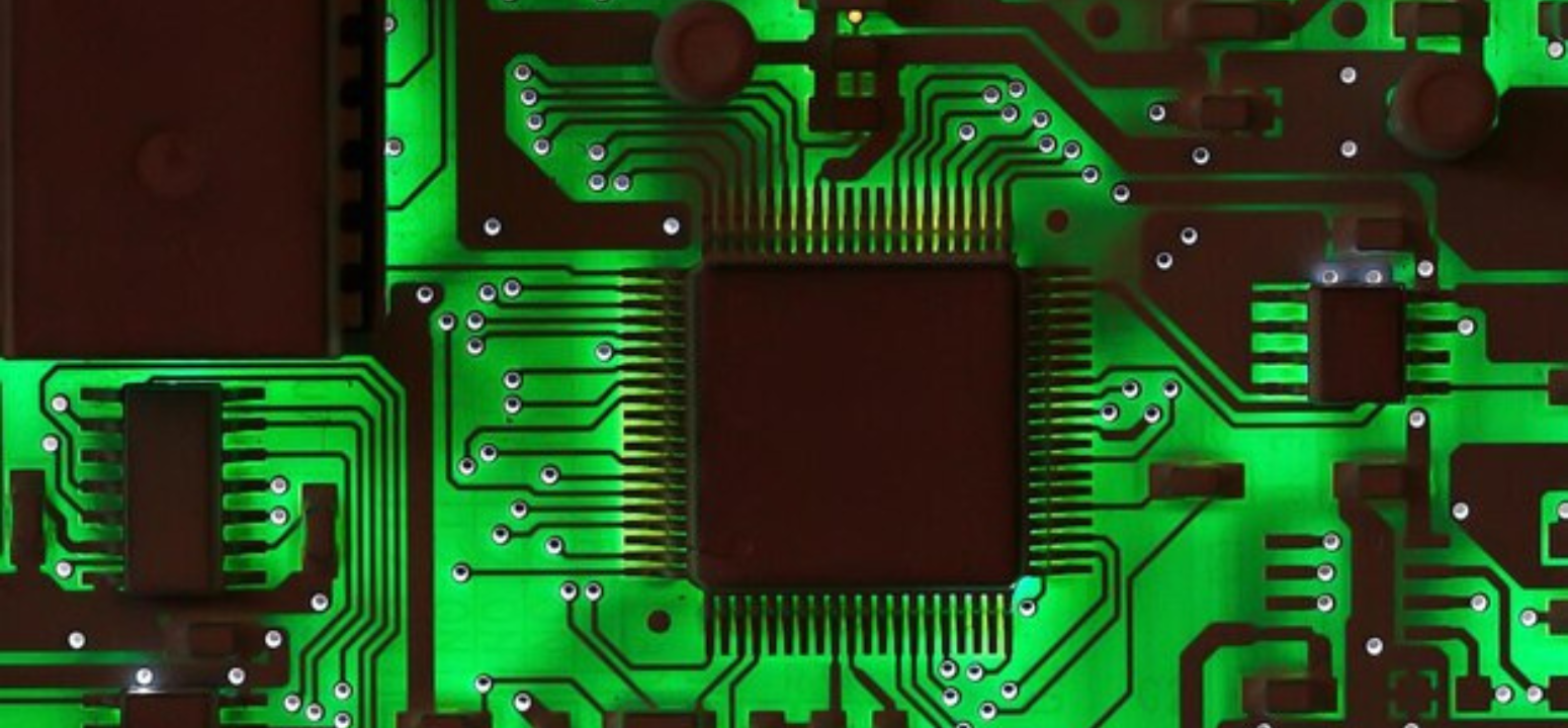
In the intricate world of Very Large Scale Integration (VLSI), the design process is a carefully orchestrated sequence of steps known as the VLSI Design Flow. This comprehensive guide will walk you through the key stages, methodologies, and challenges involved in crafting the intricate semiconductor designs that power today’s advanced electronics.
1. Conceptualization and Specification:
The journey begins with a concept – an idea that has the potential to revolutionize technology. During this phase, engineers work closely with stakeholders to define project requirements, specifications, and performance expectations. The goal is to establish a clear foundation for the design process.
2. Architectural Design:
Once the specifications are defined, architects create a high-level design that outlines the system’s architecture. This involves decisions regarding the choice of components, their interconnections, and the overall structure of the system. The focus is on functionality, performance, and scalability.
3. Logic Design:
In the Logic Design phase, the high-level architecture is translated into a logical representation using hardware description languages (HDL) like Verilog or VHDL. This step involves designing digital circuits, specifying the flow of data, and defining the control paths.
4. RTL Synthesis:
Register-Transfer Level (RTL) synthesis is a critical step where the logical representation is transformed into a netlist of gates and flip-flops. This netlist forms the basis for subsequent stages of the design flow. Tools like Synopsys Design Compiler are often employed for efficient synthesis.
5. Netlist and Floorplanning:
The generated netlist, a detailed description of the circuit’s connectivity, is used to create a physical floorplan. Floorplanning involves placing functional blocks, defining their dimensions, and establishing the physical organization of the chip.
6. Placement and Routing:
During this stage, tools like Cadence Innovus or Synopsys IC Compiler come into play. Placement involves determining the precise locations of cells on the chip, while routing deals with establishing the connections between them. Optimization algorithms are applied to enhance performance, minimize power consumption, and meet timing constraints.
7. Physical Verification:
Physical verification ensures that the design adheres to manufacturing constraints, including design rules, spacing, and other critical parameters. DRC (Design Rule Checking) and LVS (Layout versus Schematic) checks are performed to validate the physical design.
8. Timing Analysis:
Timing analysis evaluates the performance of the design by analyzing signal propagation delays and meeting specified timing requirements. This step is crucial for ensuring that the design functions reliably within specified clock cycles.
9. Extraction and Simulation:
Accurate parasitic information is extracted from the layout, and simulations are conducted to validate the design’s functionality and performance. This iterative process helps identify and address any discrepancies or issues that may arise.
10. Tapeout:
Tapeout marks the finalization of the design, where the files are sent to the semiconductor fabrication facility for mass production. This step involves creating the final set of files, including the GDSII (Graphic Data System II) file that contains the layout information.
Conclusion:
The VLSI Design Flow is a meticulous journey from conceptualization to fabrication, where innovation meets engineering precision. Each stage is interconnected, requiring expertise, collaboration, and cutting-edge tools to navigate successfully. As technology continues to advance, the VLSI Design Flow remains at the forefront of semiconductor development, shaping the future of electronics and pushing the boundaries of what’s possible in the world of integrated circuits.
To know more about VLSI Course , SuccessBridge VLSI training institute. You can begin your VLSI career by enrolling in the placement-assisted live courses available at SuccessBridge We offer various VLSI online courses. We offer VLSI Physical Design course, Design Verification course, DFT Training,Chip design course many more. Explore VLSI Courses From The Leaders In VLSI Training
Also Read: A Walkthrough VLSI Physical Design Engineer Salary In India.


